March 5, 2026. 8:00 PM.
Log 6 - On I2C
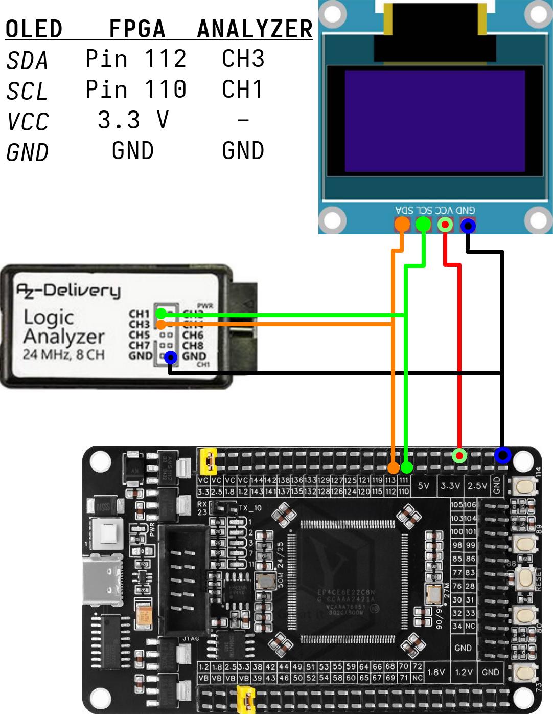
I bought a small 0.96" OLED display from Amazon for around $15. It uses the very common SSD1306 controller and has a resolution of 128x64 pixels. Electrically, the module is about as simple as it gets: it has four pins labelled VCC, GND, SCL, and SDA.
- VCC - power
- GND - ground
- SCL - serial clock
- SDA - serial data
The first two are just power. The latter two form an I2C bus, which means that if I want the FPGA to drive the display, I need to write at least a minimal I2C driver.
Before touching any HDL, I wanted to quickly review how I2C actually works. I had seen it before in a microprocessors course, but not in enough detail to sit down and implement it from scratch in FPGA logic without checking a few things first. I also skimmed some online references, including a helpful document from TI, mainly to refresh the timing rules.
I2C Basics
I2C is a simple two-wire serial communication protocol. One device on the bus acts as the master and controls the communication, while the other devices are slaves. Each slave has an address, and the master selects which device it wants to talk to by sending that address over the bus.
One of the key details is that the lines are open-drain. In practical terms, that means devices do not actively drive the bus high. Instead, they either pull the line low or let go of it. When nobody is pulling the line down, a pull-up resistor brings it back to the high level.
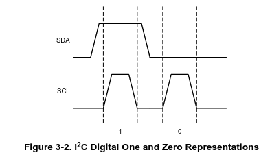
The bus has two signals:
- SDA carries the data
- SCL carries the clock
Bits are transferred one at a time on SDA and are sampled while SCL is high. For a bit to be valid, the SDA line must remain stable during that high portion of the clock pulse. In other words, you generally change the data while the clock is low, then let the receiver read it while the clock is high.
Transactions
At a higher level, communication on the bus is framed by two special conditions: START and STOP.
- A START condition occurs when SDA transitions from high to low while SCL remains high.
- A STOP condition occurs when SDA transitions from low to high while SCL remains high.
These are important because they are not ordinary data bits. They are special bus events that tell every device on the bus when a transaction is beginning and ending.
TODO: Insert START/STOP timing diagram
Data itself is sent in 8-bit chunks. After each byte, there is a ninth clock pulse used for an ACK bit. The receiving device pulls SDA low during that bit time to acknowledge that it successfully received the byte.
WRITE Transaction
A typical write transaction looks roughly like this:
- START condition
- 7-bit slave address
- Read/write bit
- ACK from slave
- One or more data bytes
- ACK after each byte
- STOP condition
READ Transaction
A read transaction follows the same general pattern, except that after the address phase the slave drives the data line and the master acknowledges the received bytes.
TODO: Insert general I2C read/write transaction diagram from notes
What I Need to Implement
In theory, the FPGA side of this breaks down into a few basic operations:
- Generate a START condition
- Transmit one bit at a time on SDA
- Pulse SCL correctly for each bit
- Release SDA and read back the ACK bit
- Generate a STOP condition
That sounds simple enough on paper, but in HDL it is a bit different from writing software for a microcontroller. On a microcontroller, you might imagine having separate functions for "start", "stop", "send bit", and "read ACK", and just calling them one after another. In FPGA logic, that behaviour has to be built explicitly over time, which means this will almost certainly end up as an FSM that steps through each phase of the protocol one clock cycle at a time.
The Problem
So the first milestone is intentionally very small: I do not need to write a full display driver yet. I just need to prove that the FPGA can begin an I2C transaction properly and that the OLED responds.
Consequently, the first test should be:
- Generate a START condition
- Send the OLED address
- Read back the ACK bit
If I can see that ACK, either internally on the FPGA or externally on the logic analyzer, then the bus timing is at least sane and the basic driver structure is working. Once that part is reliable, sending actual commands and data to the display becomes much more straightforward.
Wiring
I connected the OLED to the FPGA and the Logic Analyzer following the diagram below:
Program Architecture
In my 5th semester, I wrote an assembly language driver for a line-following robot [TODO: link to follow] that involved a similar structure to communicate with the on-board LCD. It had a multi-level structure, where each level would be responsible for a different abstraction of the protocol. I decided to take a similar approach in this project:
- (L1) Bit Engine: Manipulates the relevant busses at a primitive/timing level.
- (L2) Byte Engine: Handles byte-level operations, commands the L1 Bit Engine with primitive conditions (S, P, etc.) and data bytes.
- (L2) Tick Generator: Generates timing ticks for the I2C protocol.
- (L3) I2C Master Program: Knows transaction structure, tells the L2 byte engine which commands to run.
- (L4) Top Level Program: Runs the entire code, including the L3 I2C Master Program.
[L1] Bit Engine
i2c_bit_engine This is the lowest-level timed line driver. It should receive commands like 'drive SDA LO', 'release SCL', 'sample SDA', etc. It should also wait for a shared tick to occur, and step through these tiny timing phases. It's dumb and reusable, and doesn't know anything about anything WRT addresses, bytes, or transactions. It's no more than a simple tool for higher levels to use.[L2] Byte Engine
i2c_byte_engine This is the next level up, and where START/STOP/WRITE_BIT/READ_BIT should live. This module should generate the S/P primitive states, be able to write and read bits using the i2c_bit_engine. It should also be able to take in a byte and write it out bit by bit, and read in a byte bit by bit and return it. Finally, it should be able to handle the ACK bit.[L2] Tick Generator
i2c_tick_generator This module generates the timing ticks for the I2C protocol. It should be able to run at a configurable speed, and generate a tick at the appropriate intervals. The i2c_bit_engine will use this tick to step through its timing phases.[L3] I2C Master
i2c_master This is the highest level of the driver, and should know how to structure transactions. It takes in a transaction intent, and commands the i2c_byte_engine based on that.[L4] Top Level Program
top This is the top level of the design, and should run the entire program. It decides what to do and when, and commands the i2c_master to execute transactions based on that. For this first test, the program should just run one transaction to send the OLED address and read back the ACK, then stop.SV L2 Tick Generator Implementation
I first decided to implement the L2 Tick Generator, since the Bit Engine will need it to run. For this, I made the following 2 files:
/rtl/i2c/i2c_tick_generator.sv
/hw_tests/i2c/tick_test_top.sv
The tick generator is pretty straightforward:
i2c_tick_generator.sv
The tick generator tester was also pretty simple:
tick_test_top.sv
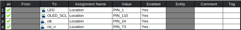
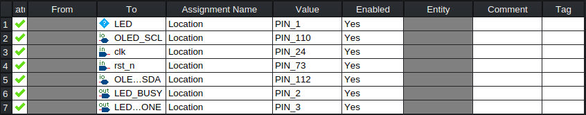
Pin Assignments
I set the tick_test_top.sv as the top_level entity, and synthesized it to confirm no errors. Then, I added some pin assignments to connect the tick output to both the LED and the SCL-connected pin to the FPGA.
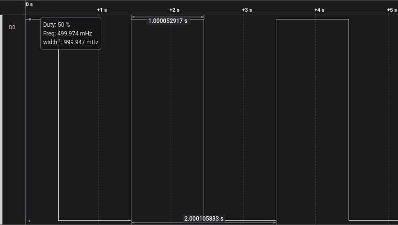
Result
I then ran the test on the FPGA, and visually observed the LED blinking at a steady rate, which was a good sign. I also opened my logic analyzer software, and confirmed that the SCL line (CH1) had a square waveform with a frequency of 2 Hz - this means the 'tick' would pulse at a rate of 1 Hz. Excellent!
SV L1 Bit Engine Implementation
With the tick generator working, I moved onto the L1 Bit Engine. This is the lowest-level timed line driver. It does not know anything about bytes, or transactions, or anything of the sort. It should only know how to perform a single timed bus micro-step on SDA/SCL. It's job is basically:
- Drive SDA low or high (release)
- Drive SCL low or high (release)
- Sample SDA
- Wait for a tick from the tick generator
- Say "done"
/rtl/i2c/i2c_bit_engine.sv
/hw_tests/i2c/bit_engine_test.sv
The bit generator structure is pretty straightforward:
The file I made for the bit engine generator is below:
i2c_bit_generator.sv
To test the bit generator, I had to test 4 states:
- Release SDA, SCL
- SDA LO, SCL HI
- SDA LO, SCL LO
- SDA HI, SCL LO
tick_test_top.svPin Assignments
I set the bit_engine_test.sv as the top_level entity, and synthesized it to confirm no errors. Then, I added some pin assignments to connect the tick output to both the LED and the SCL-connected pin to the FPGA.
Result
Let's take a look at the waveform output from the logic analyzer when I ran this test. The channels are as follows:
- CH1 (D0): SCL
- CH3 (D2): SDA
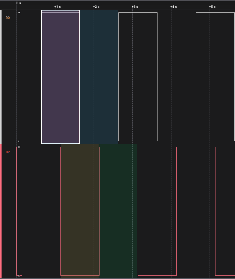 Looks like the state transitions work properly. In the first state, both lines are released (high). In the second state, SDA is low and SCL is high. In the third state, both lines are low. In the fourth state, SDA is high and SCL is low. The cycle then repeats. Excellent!