March 15, 2026. 12:00 PM.
Log 7 - On I2C, Part 2
In the previous log, I had planned out and started work on an I2C driver for my OLED display. I started by implementing the L2 Tick Generator, which produces timing ticks for the I2C protocol. After confirming that it worked correctly, I moved on to the L1 Bit Engine, which is responsible for driving the SDA and SCL lines according to the I2C timing requirements.
The L2 Byte Engine
The L2 Byte Engine is responsible for byte-level operations, commanding the L1 Bit Engine with primitive conditions (S, P, etc.) and data bytes. I decided to implement it as an FSM that steps through the various phases of each I2C primitive. The implemented states are:
- IDLE
- START
- STOP
- WRITE_BIT
- READ_BIT
- WRITE_BYTE
- AWAIT_ACK
In a stroke of convenience, I realised each operation corresponds to basically 3 states: State before, state during, state after. As such, the FSM structure is pretty straightforward. For example, for the START condition:
- State Before: Release SDA, SCL
- State Before, WAIT: Wait for operation to complete
- State During: Drive SDA LO, keep SCL HI
- State During, WAIT: Wait for operation to complete
- State After: Keep SDA LO, drive SCL LO
- State After, WAIT: Wait for operation to complete. Return to State = IDLE.
Et c'est tout! Pretty simple. The other bit-wise operations follow the same general pattern, just with different line-driving behaviour. Of course, I have the byte-write operation, which has to loop through each bit, then wait for an ACK bit. As such, the FSM looks like this:
- ST_WBYTE_LOAD: Load the byte to be written into the shift register. Set the index to 7 (indices are 7..0).
- ST_WBYTE_B0: Drive SCL LO while driving the SDA to be the value of the MSB of the shift reg.
- ST_WBYTE_B0W: Wait for operation to complete
- ST_WBYTE_B1: Release SCL, keeping SDA the required data value
- ST_WBYTE_B1W: Wait for operation to complete
- ST_WBYTE_B2: Drive SCL LO, keeping SDA the required data value
- ST_WBYTE_B2W: Wait for operation to complete. Then, check the bit index. If it's 0 (last bit), update state to AWAIT_ACK. Otherwise, shift the shift register 1 bit to the left and lower the index by 1. Finally, set the state back to ST_WBYTE_B0.
The AWAIT_ACK state is last. We need to release SDA and pulse SCL to read the ACK bit from the slave. If the slave pulls SDA LO, then we know the byte was successfully received. If the slave doesn't touch SDA, we know the byte wasn't received and we can handle that as well [TODO: implement this!].
- ST_ACK_0: Drive SCL LO while releasing SDA
- ST_ACK_W0: Wait for operation to complete
- ST_ACK_1: Release SCL while keeping SDA HI. Request a sample of the bit using bit_sample_req.
- ST_ACK_W1: Wait for operation to complete. Once done, set rx_bit to the sampled value, and ack_ok to the inverse of the sampled value. Why? because if we sample LO on the SDA line, then the ACK was successful. Otherwise, we've got a problem that needs handling. I'll implement error handling code later, once I've got a confirmed test here.
- ST_ACK_2: Drive SCL LO while releasing SDA
- ST_ACK_W2: Wait for the operation to complete
That leaves us with a grand total of 37 states (!!!) for our FSM.
/rtl/i2c/i2c_byte_engine.sv
Now, let's write a test file for this byte engine and see if it works. We need to test the various primitives first, then we can move on to testing byte writes. Let's start with the primitives. I wrote an SV test file that commands the byte engine to execute just the S and P conditions, and used my logic analyzer to confirm. But that's not the big test here. I have to check if, when i write a byte with the address of the OLED display, the correct sequence of bits is sent out over the SDA line, and (biggest test) the ACK bit is correctly received. So, I wrote a test that commands the byte engine to write the byte 0x78 (which is the 7-bit I2C address of the OLED display, left-shifted by 1 bit to account for the R/W bit, which is set to 0 for write) and observed the following on the logic analyzer.
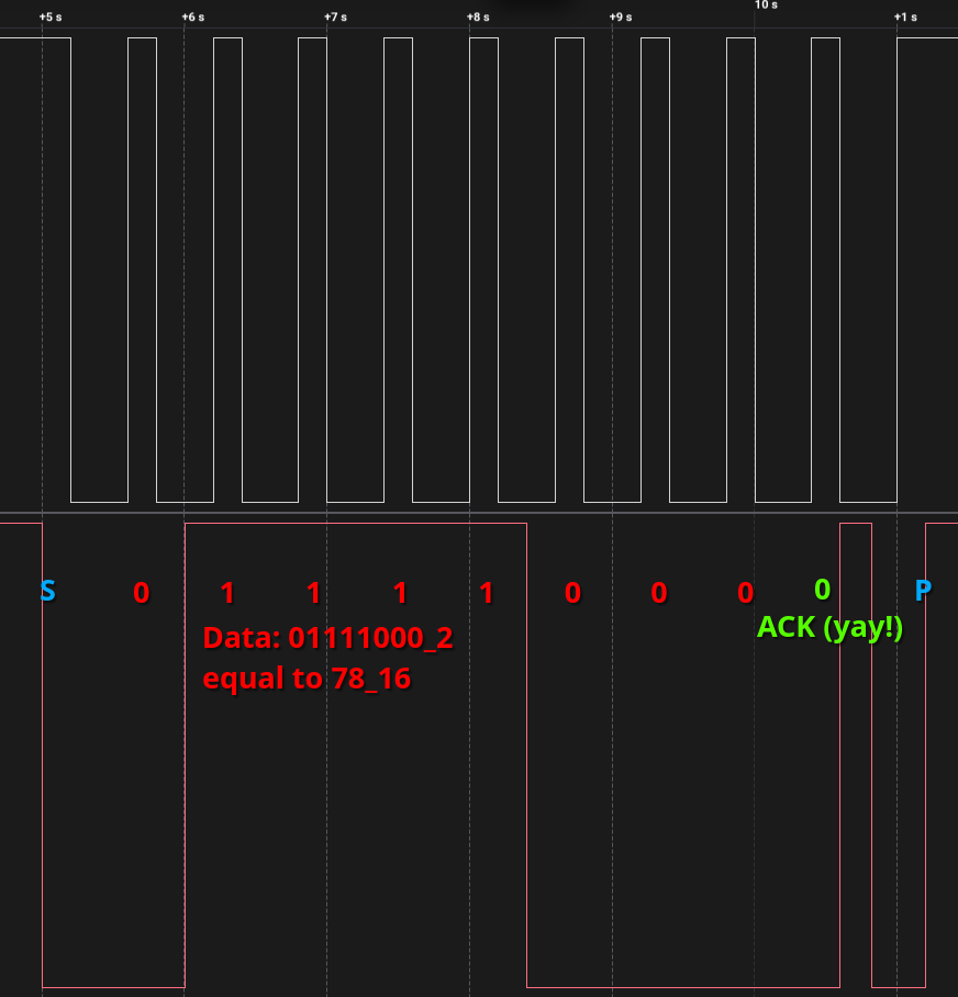
IT LIVES!!! The capture shows a proper S and P condition, with the correct timing. The byte is correctly transmitted, and, most excitingly, the ACK bit is correctly received! This is a major milestone for this project, as it means the core functionality of the I2C driver is working. Next steps, for the next log, will be to implement the higher-level operations.